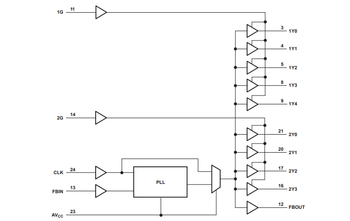
CDCVF2509 is a high performance, low tilt, low jitter, phase locked loop (PLL) clock driver. It uses a PLL to precisely align the feedback (FBOUT) output to the clock (CLK) input signal at both frequency and phase. It is specifically designed for synchronous dram.
Block diagram

CDCVF2509 works at 3.3v VCC. It also offers integrated series damping resistors, making it ideal for driving point-to-point loads. A five-output group and a four-output group provide nine low-tilt, low-jitter copies of the CLK. The duty cycle of the output signal is adjusted to 50%, which has nothing to do with the duty cycle of CLK. Each set of outputs is enabled or disabled by the control (1G and 2G) inputs, respectively. When G input is high, the output switches with CLK in phase and frequency. When the G input is low, the output is disabled to the logical low state.
Shape of package

Unlike many products that contain PLL, the CDCVF2509 does not require an external RC network. The loop filter of the PLL is included on the chip, minimizing the number of components, board space, and cost.