IR2112S Introduction
The IR2112S is a high-speed, high-voltage driver designed for power MOSFETs and IGBTs, featuring independent high and low side output channels. Its rugged monolithic construction is made possible by proprietary HVIC and latch-immune CMOS technologies, ensuring reliability in demanding applications.
The driver is compatible with standard CMOS or LSTTL logic inputs, including 3.3V logic, and incorporates a high pulse current buffer stage to minimize cross-conduction. With matched propagation delays, the IR2112S is ideal for high-frequency applications, and its floating channel supports driving N-channel MOSFETs or IGBTs on the high side, with a maximum voltage rating of 600V.
IR2112S Pinout

VDD: Logic supply
HIN: Logic input for high side gate driver output (HO), in phase
SD: Logic input for shutdown
LIN: Logic input for low side gate driver output (LO), in phase
VSS: Logic ground
VB: High side floating supply
HO: High side gate drive output
VS: High side floating supply return
VCC: Low side supply
LO: Low side gate drive output
COM: Low side return
IR2112S Symbol

IR2112S Footprint

IR2112S 3D Model

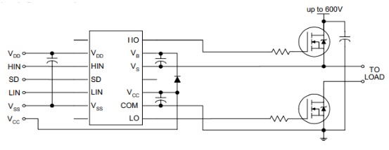
IR2112S Typical Connection

IR2112S Functional Block Diagram

IR2112S Specification
| Specification | Value |
| Device Type | IGBT, N-Channel MOSFET |
| Number of Drivers | 2 |
| Supply Voltage | 10V ~ 20V |
| Logic Voltage - VIL, VIH | 6V, 9.5V |
| Peak Output Current | 250mA, 500mA |
| Pulse Current Buffer Stage | Designed for minimal cross-conduction |
| Propagation Delay | Matched delays for high-frequency applications |
| Floating Channel | Can drive N-channel MOSFETs or IGBTs in high-side configuration |
| High Side Output Voltage | 600 V |
| Rise / Fall Time | 80ns, 40ns |
| Operating Temperature | -40°C ~ 150°C |
| Package | 16-SOIC |
IR2112S Features
Floating channel designed for bootstrap operation
Fully operational to +600V
Tolerant to negative transient voltage dV/dt immune
Gate drive supply ranges from 10 to 20V
Undervoltage lockout for both channels
3.3V logic compatible
Separate logic supply range from 3.3V to 20V
Logic and power ground ±5V offset
CMOS Schmitt - triggered inputs with pull-down
Cycle by cycle edge-triggered shutdown logic
Matched propagation delay for both channels
Outputs in phase with inputs
IR2112S Applications
Motor Drives
DC-AC Inverters
Switching Power Supplies
Induction Heating
Lighting Control Systems
Power Conversion Systems
Electric Vehicles (EVs)
Hybrid Electric Vehicles (HEVs)
IR2112S Package
The IR2112S comes in a 16-SOIC package, offering a compact and efficient solution for high-speed power MOSFET and IGBT driving applications. The package dimensions are 10.3mm x 5.3mm x 1.75mm (length x width x height), with a standard lead pitch of 1.27mm. This surface-mount package is designed to provide excellent thermal and electrical performance while saving space on PCBs, making it ideal for high-performance industrial and motor control systems.

How to Use IR2112S?
1. First, connect the VDD pin to the appropriate logic power supply and ground the VSS pin. Next, provide low-side power to VCC and COM, usually at the same voltage as VDD, ensuring a stable ground reference for both VSS and COM.
2. Input the appropriate logic signals to HIN and LIN, which determine the operation of the high-side and low-side switches. Ensure the signal levels on HIN and LIN are correct. Using these pins, you can control the switching of HO and LO outputs.
3. Use the SD pin to enable or disable the functionality. To shut down the system, pull the SD pin low, which disables both high-side and low-side outputs, ensuring a safe system stop. Conversely, pulling the SD pin high will restore the drive functionality.
4. Connect the high-side devices through VS and VB pins. These pins support driving high-side MOSFETs or IGBTs while maintaining isolation from the low-side power. You can monitor the high-side output through the HO pin, while the LO pin is used to control the switching of the low-side device.
FAQs
How do I prevent cross-conduction in the IR2112S?
The IR2112S features a high-pulse current buffer stage designed to minimize cross-conduction between the high-side and low-side drivers, ensuring efficient and safe operation, especially in high-speed applications.
What are the typical applications of the IR2112S?
The IR2112S is commonly used in motor drives, switching power supplies, DC-AC inverters, and other high-voltage applications that require efficient and reliable gate driving for power MOSFETs or IGBTs.
What logic levels are compatible with the IR2112S inputs?
The IR2112S logic inputs (HIN, LIN, SD) are compatible with 3.3V logic or LSTTL levels, which ensures compatibility with modern microcontrollers or other logic circuits.