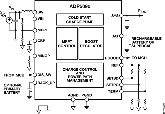
The ADP5090 is an integrated boost regulator that converts dc power from PV cells or TEGs. The device charges storage elements such as rechargeable Li-Ion batteries, thin film batteries, super capacitors, and conventional capacitors, and powers up small electronic devices and battery-free systems.
The ADP5090 provides efficient conversion of the harvested limited power from a 16 µW to 200 mW range with sub-µW operation losses. With the internal cold-start circuit, the regulator can start operating at an input voltage as low as 380 mV. After cold startup, the regulator is functional at an input voltage range of 80 mV to 3.3 V.
By sensing the input voltage at the VIN pin, the control loop keeps the input voltage ripple in a fixed range to maintain stable dc-to-dc boost conversion. The VIN OCV sensing and programmable regulation points of the input voltage allow extraction of the highest possible energy from the PV cell or TEG harvester. A programmable minimum operation threshold (MINOP) enables boost shutdown during a low light condition. In addition, the DIS_SW pin can temporarily shut down the boost regulator and is RF transmission friendly.
The charging control function of ADP5090 protects rechargeable energy storage, which is achieved by monitoring the battery voltage with programmable charging termination voltage and shutdown discharging voltage. In addition, a programmable PGOOD flag monitors the SYS voltage.
An optional primary cell battery can be connected and managed by an integrated power path management control block that automatically switches the power source from the energy harvester, rechargeable battery, and primary cell battery.
The ADP5090 is available in a 16-lead, 3 mm × 3 mm LFCSP package and is rated for a −40°C to +125°C junction temperature range.
| Référence | Description | |
|---|---|---|
| ADP5090ACPZ-1-R7 Analog Devices Inc. |
PMIC - Chargeurs batteries, IC REG BOOST 1V 16LFCSP | RFQ |
| ADP5090ACPZ-2-R7 Analog Devices Inc. |
PMIC - Chargeurs batteries, IC REG BOOST 1V 16LFCSP | RFQ |
Traction inverters are the main battery drain components in electric vehicles (EVs), with power levels up to 150kW or higher. The efficiency and performance of traction inverter directly affect the driving range of electric vehicle after a single charge. Therefore, in order to build the next generation of traction inverter systems, silicon carbide (SiC) field effect transistor (FET) is widely used in the industry to achieve higher reliability, efficiency and power density.
Do you know the 8 application circuits of operational amplifiers?
This technical presentation requires an understanding of how to configure an operational amplifier in a typical gain control circuit. The applications of linear and nonlinear digital potentiometers are discussed. This article gives an overview of the basic techniques required to convert audio and other potentiometer/op amp applications from conventional mechanical potentiometers to solid state potentiometers
The current in an electronic circuit usually has to be limited. In USB ports, for example, excessive current must be prevented to provide reliable protection for the circuit. Also in the power bank, the battery must be prevented from discharging. Too high discharge current results in too large voltage drop of the battery and insufficient supply voltage of downstream devices
Using advanced real-time control technologies such as motor control circuits with higher power density, higher integration and more efficient systems, better acoustic performance of the system can be achieved
Brushless direct current (BLDC) motors have been widely used in household appliances, industrial equipment and automobiles. While brushless DC motors offer a more reliable and maintainable alternative to traditional brushless motors, they require more sophisticated electronics to drive them
How to achieve precise motion control in industrial actuators
The NCP51820 is a 650 V, high-speed, half-bridge driver capable of driving gallium nitride (" GaN ") power switches at dV/dt rates up to 200 V/ns. The full performance advantages of high voltage, high frequency and fast dV/dt edge rate switches can only be realized if the printed circuit board (PCB) can be properly designed to support this power switch. This paper will briefly introduce NCP51820 and the key points of PCB design of high performance GaN half bridge grid driver circuit using NCP51820